Semiconductor Wafer Fabrication Equipment: Guide to Processes and Practical Insights
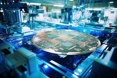
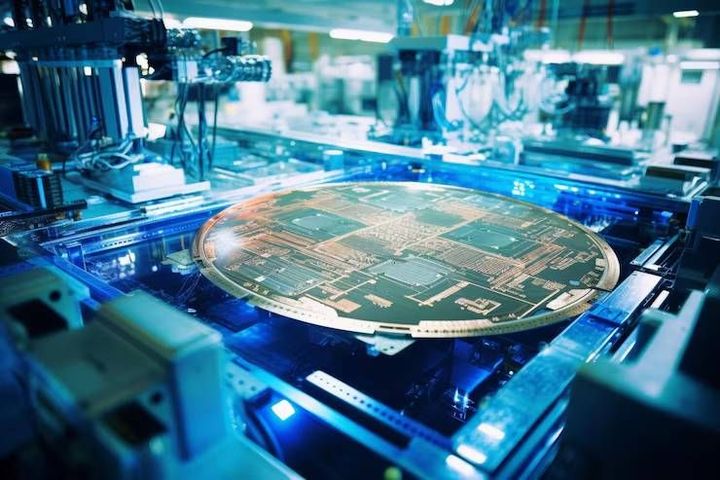
Semiconductor Wafer Fabrication Equipment refers to the specialized machines used to transform semiconductor wafers into integrated circuits and other electronic devices. These machines perform highly controlled processes such as cleaning, coating, lithography, deposition, etching, ion implantation, polishing, inspection, and thermal processing.
A semiconductor wafer is a thin, circular slice of material, commonly silicon, that acts as the foundation for many electronic devices. During fabrication, layers of different materials are repeatedly added, patterned, modified, and removed to create microscopic structures.
Modern fabrication facilities, commonly called fabs, contain many types of equipment operating together under carefully controlled environmental conditions. SEMI identifies wafer processing, fab facilities, and mask or reticle equipment as major parts of the wafer fabrication equipment ecosystem.
How Wafer Fabrication Works
Semiconductor manufacturing involves many repeated process cycles. A simplified sequence includes:
Wafer preparation: Silicon wafers are cleaned and prepared for processing.
Oxidation or deposition: Thin material layers are formed on the wafer.
Photoresist coating: A light-sensitive material is applied to the surface.
Lithography: A pattern is transferred onto the photoresist using controlled light or another exposure method.
Development: Selected portions of the photoresist are removed to reveal the underlying pattern.
Etching: Exposed material is selectively removed.
Ion implantation: Selected regions are modified by introducing controlled ions.
Thermal processing: Heat is used for oxidation, activation, diffusion, or other material changes.
Chemical mechanical polishing: The surface is polished to achieve controlled flatness.
Cleaning: Contaminants and unwanted materials are removed between processing stages.
Inspection and metrology: Equipment checks dimensions, layers, defects, particles, and other characteristics.
These steps may be repeated many times as increasingly complex structures are built on the wafer. SEMI's wafer-fabrication training materials identify processes including lithography, etching, ion implantation, chemical vapor deposition, physical vapor deposition, thermal processing, cleaning, and chemical mechanical polishing as major fabrication technologies.
Major Equipment Categories
Lithography equipment transfers circuit patterns onto a wafer. Exposure systems, aligners, scanners, and related track equipment are used for different stages of pattern formation.
Deposition equipment creates thin layers of material. Chemical vapor deposition, physical vapor deposition, atomic layer deposition, and related techniques can be used depending on the required material and structure.
Etching equipment removes selected material from the wafer. Both dry and wet etching technologies are used in semiconductor fabrication.
Ion implantation equipment introduces selected ions into specific wafer regions to modify their electrical characteristics.
Thermal processing equipment uses controlled heating and cooling for processes such as oxidation, annealing, and dopant activation.
Cleaning equipment removes particles, chemical residues, and other contaminants from wafer surfaces.
Chemical mechanical polishing equipment combines chemical reactions and mechanical polishing to create controlled surface conditions.
Inspection and metrology equipment measures dimensions, thickness, alignment, surface conditions, particles, and defects.
Importance
Building Complex Electronic Devices
Semiconductor Wafer Fabrication Equipment enables the creation of extremely small structures across a wafer surface. Modern chips may contain very large numbers of interconnected components formed through repeated manufacturing steps.
The accuracy of each process influences subsequent stages. A small variation in layer thickness, pattern position, contamination level, or etching behavior can affect the final device.
Controlling Manufacturing Precision
Fabrication equipment must maintain carefully controlled parameters such as temperature, pressure, chemical concentration, gas flow, exposure conditions, plasma characteristics, and mechanical movement.
Different machines perform different functions, but they must work together as part of a controlled manufacturing sequence.
Managing Contamination
Particles and unwanted chemical contamination can interfere with microscopic structures. Semiconductor fabs therefore use controlled environments, specialized filtration, wafer-handling systems, cleaning equipment, and monitoring technologies.
Cleanroom design is particularly important because fabrication dimensions can be much smaller than ordinary visible particles.
Supporting Different Chip Technologies
Equipment configurations vary according to the semiconductor technology being produced. Logic processors, memory devices, power semiconductors, sensors, radio-frequency components, and other devices can require different process flows.
The required equipment can also change as manufacturers introduce new materials, transistor structures, interconnect technologies, and packaging approaches.
Major Equipment and Functions
| Equipment Category | Main Function | Typical Process |
|---|---|---|
| Lithography system | Transfers patterns | Pattern formation |
| Deposition system | Adds thin material layers | CVD, PVD, ALD |
| Etch system | Removes selected material | Dry or wet etching |
| Ion implanter | Modifies wafer regions | Doping |
| Thermal processor | Controls material properties | Annealing, oxidation |
| CMP system | Planarizes surfaces | Polishing |
| Cleaning system | Removes contaminants | Wafer cleaning |
| Metrology system | Measures wafer characteristics | Thickness and dimensions |
| Inspection system | Detects defects and particles | Process monitoring |
Recent Updates
Growth in Semiconductor Equipment Investment
Semiconductor equipment investment has continued to expand as manufacturers increase capacity for advanced computing, memory, and other electronic applications. SEMI reported that worldwide semiconductor manufacturing equipment billings reached approximately $135.1 billion in 2025, a 15% increase from 2024. Wafer processing equipment sales increased by 12% during the same period.
SEMI has also reported that artificial intelligence demand is contributing to investment in advanced logic, memory, and high-bandwidth memory production.
Advanced Lithography
Lithography remains one of the most technically demanding areas of wafer fabrication. Modern semiconductor manufacturing uses sophisticated exposure systems to create increasingly small patterns.
Advanced lithography is closely connected with developments in optics, photoresists, masks, computational techniques, wafer positioning, and process control. Different semiconductor nodes can use combinations of exposure technologies rather than relying on one technique for every layer.
More Advanced Deposition and Etching
As device structures become more complex, manufacturers increasingly require precise control over thin-film formation and material removal.
Atomic layer deposition can create extremely thin and conformal layers through repeated surface reactions. Advanced plasma etching can selectively remove material from complicated structures while controlling profile and surface characteristics.
SEMI's semiconductor equipment categories include CVD, PVD, ALD, dry etching, wet etching, stripping, and related process technologies.
AI and Process Control
Artificial intelligence and machine-learning techniques are increasingly being explored for equipment monitoring, defect classification, process analysis, predictive analysis, and manufacturing optimization.
These systems can analyze large quantities of information generated by sensors and inspection equipment. Their usefulness depends on data quality, process understanding, validation, and appropriate human oversight.
Advanced Memory and AI Hardware
Demand for AI computing has increased investment in advanced logic and memory manufacturing. High-bandwidth memory has become particularly important for high-performance computing architectures.
SEMI reported that 2025 equipment investment was supported by expansion in advanced logic and memory capacity, while test and packaging equipment also experienced substantial growth.
Expansion of Semiconductor Manufacturing in India
India is developing its semiconductor manufacturing ecosystem through the India Semiconductor Mission and related government programs. MeitY's 2025–26 annual report states that approved initiatives include semiconductor fabrication facilities, assembly and testing facilities, design support, and modernization of the Semiconductor Laboratory in Mohali.
The same report describes the modernization of the 200 mm, 180 nm CMOS line at Semiconductor Laboratory, with planned capacity and capability improvements.
Laws or Policies
International Semiconductor Controls
Semiconductor manufacturing equipment is affected by technology regulations and export-control frameworks in several countries. These rules can restrict the transfer of certain advanced manufacturing equipment, software, technologies, and related components to particular destinations or end users.
For example, the U.S. Bureau of Industry and Security maintains regulations covering semiconductor manufacturing equipment and related technologies. Its rules include controls involving specified semiconductor manufacturing equipment and equipment used for advanced integrated-circuit production.
Export-Control Developments
Export controls have become increasingly relevant to semiconductor equipment supply chains. In 2025, the U.S. Department of Commerce announced changes affecting foreign-owned semiconductor fabs in China and their ability to receive certain U.S.-origin equipment and technology without licenses.
In 2026, BIS also announced a major settlement concerning unauthorized exports of semiconductor manufacturing equipment to China.
These developments demonstrate that semiconductor equipment procurement can involve technical, legal, geographic, and end-use considerations.
India's Semiconductor Policy
India's semiconductor policy framework includes fiscal support for establishing silicon-based semiconductor fabrication facilities. MeitY documentation describes a scheme providing support equal to 50% of eligible project expenditure for silicon semiconductor fabs, subject to the applicable program conditions.
The framework also includes support for compound semiconductors, silicon photonics, sensors, discrete semiconductor facilities, and semiconductor assembly and testing activities.
Environmental and Workplace Requirements
Semiconductor fabs use specialized chemicals, gases, water systems, electrical infrastructure, cleanroom equipment, and high-precision machinery. Consequently, facilities must consider environmental protection, chemical handling, worker safety, waste management, emissions, water management, and emergency procedures.
The specific requirements vary by country and facility type. Local environmental, occupational, electrical, building, chemical, and hazardous-material regulations may all apply.
Tools and Resources
Process Simulation Software
Semiconductor process simulation tools can model selected fabrication steps before physical processing. They can help engineers examine variables such as deposition, etching, implantation, thermal treatment, and device characteristics.
Metrology Systems
Metrology equipment measures physical and material characteristics of wafers. Common measurements include film thickness, critical dimensions, surface characteristics, alignment, electrical properties, and wafer flatness.
Inspection Systems
Inspection platforms use optical, electron-beam, or other techniques to identify particles, pattern defects, surface irregularities, and other manufacturing issues.
Cleanroom Monitoring
Cleanroom monitoring systems track environmental conditions such as airborne particles, temperature, humidity, pressure differences, and other parameters relevant to fabrication.
Equipment Monitoring
Modern fabrication equipment contains sensors and control systems that generate information about machine conditions. Monitoring platforms can analyze temperature, pressure, power, vibration, gas flow, and other process variables.
Industry Resources
SEMI provides information covering semiconductor manufacturing technologies, equipment categories, facilities, standards, workforce development, and industry data. Its equipment classifications include cleaning, deposition, etching, lithography, ion implantation, thermal processing, polishing, inspection, and metrology.
The India Semiconductor Mission also provides educational resources for understanding semiconductor technology. Its introductory learning platform is designed for beginners and covers fundamental semiconductor concepts.
FAQs
What is Semiconductor Wafer Fabrication Equipment?
Semiconductor Wafer Fabrication Equipment includes specialized machines used to process semiconductor wafers through steps such as lithography, deposition, etching, implantation, cleaning, polishing, thermal processing, inspection, and measurement.
How does semiconductor wafer fabrication work?
Semiconductor wafer fabrication uses repeated cycles of adding, patterning, modifying, removing, cleaning, and measuring materials on a wafer. These cycles gradually create the structures required for an integrated circuit.
What equipment is used for semiconductor wafer fabrication?
Common equipment includes lithography systems, deposition machines, etching systems, ion implanters, thermal processing systems, cleaning equipment, chemical mechanical polishing systems, inspection tools, and metrology equipment.
Why is lithography important in semiconductor fabrication?
Lithography transfers extremely precise patterns onto a wafer. These patterns define structures that later become part of transistors, interconnects, and other elements of an integrated circuit.
What are the recent trends in Semiconductor Wafer Fabrication Equipment?
Important trends include greater equipment investment, advanced lithography, more precise deposition and etching, AI-assisted process analysis, advanced memory production, improved inspection, and expansion of semiconductor manufacturing capacity in several regions.
Conclusion
Semiconductor Wafer Fabrication Equipment forms the technological foundation of modern chip manufacturing. Lithography, deposition, etching, implantation, cleaning, polishing, thermal processing, inspection, and metrology systems work together through highly controlled manufacturing sequences. Recent developments include increasing investment related to AI and advanced memory, more sophisticated process-control technologies, and semiconductor manufacturing expansion across multiple regions. Understanding these equipment categories and their roles provides a practical foundation for understanding how semiconductor wafers become the building blocks of modern electronic devices.